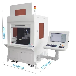
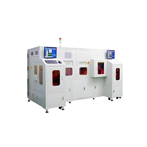
The semiconductor industry is undergoing a paradigm shift. As devices become smaller, faster, and more power-efficient, the traditional methods of wafer separation—specifically mechanical blade dicing—are reaching their physical limits. Enter the Semiconductor Wafer Laser Dicing System, a technology that has become the backbone of modern microelectronics manufacturing. Globally, the demand for laser dicing is skyrocketing, driven by the proliferation of 5G technology, electric vehicles (EVs), and Artificial Intelligence (AI) data centers.
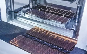
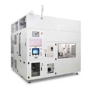
In the current industrial scenario, silicon is no longer the only king. Wide-bandgap materials like Silicon Carbide (SiC) and Gallium Nitride (GaN) are essential for high-voltage applications. However, these materials are incredibly brittle and hard, making them almost impossible to cut efficiently with traditional saws without causing significant chipping or yield loss. Laser dicing systems provide a non-contact, high-speed solution that minimizes the Heat Affected Zone (HAZ), ensuring that the integrity of the microscopic circuits remains intact.
One of the most significant trends is the adoption of Stealth Dicing. By focusing the laser beam inside the wafer substrate rather than on the surface, we create a specialized modified layer. This allows for zero-width kerfs and maximizes the number of chips per wafer (UPH - Units Per Hour).
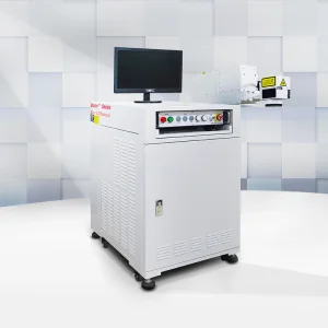
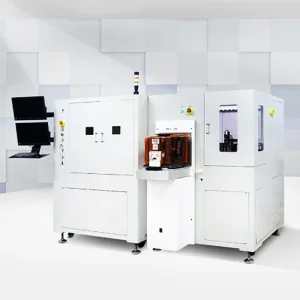
Our factory specializes in Green Laser (532nm) and UV Laser (355nm) systems. UV lasers, in particular, offer "cold processing," which is vital for delicate low-k dielectric layers and thin wafers used in 3D packaging.
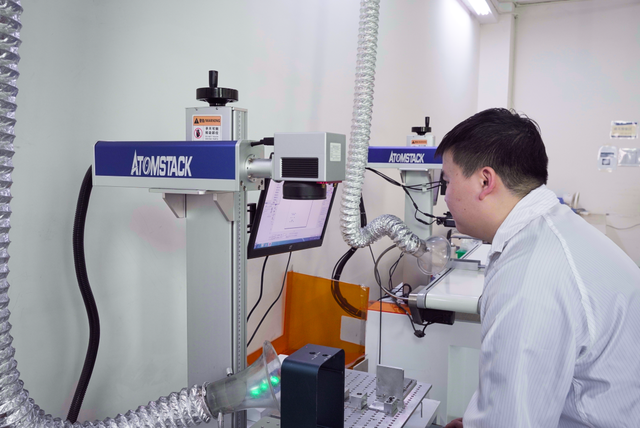
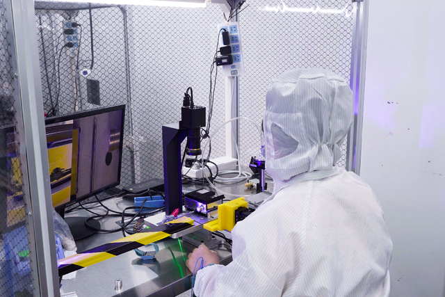
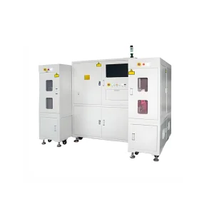
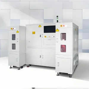
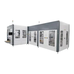
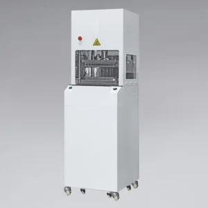
Modern systems are no longer just "cutters." They are intelligent robots equipped with CCD Vision Systems and AI algorithms for real-time alignment, kerf inspection, and automatic defect compensation, drastically reducing the need for human intervention.
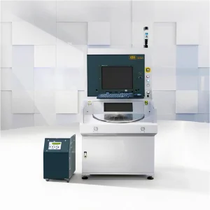
Global procurement teams from North America, Europe, and Southeast Asia are increasingly looking for partners who can offer not just a machine, but a complete ecosystem. This includes wafer cleaning, sorting, and marking. As a leading exporter, we ensure our systems are compatible with SEMI standards, allowing for seamless integration into existing Fab (fabrication) lines.
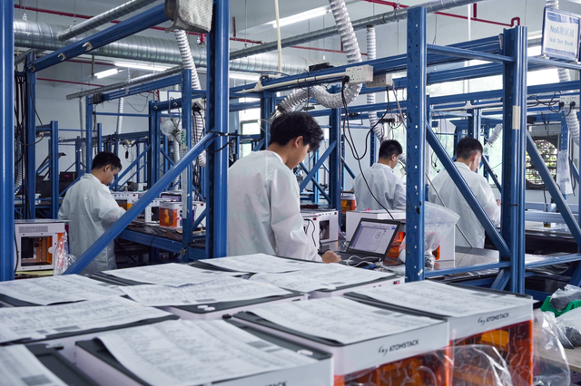
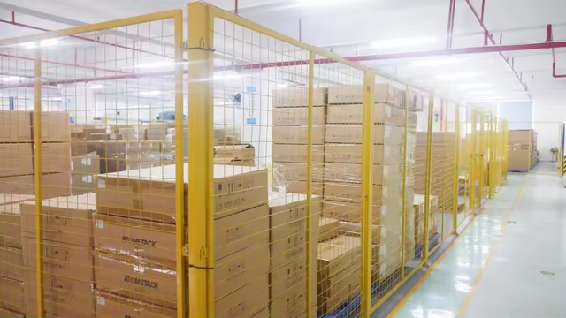
As a prominent Chinese manufacturer, Foshan Stylo Laser Co., Ltd. represents the pinnacle of "Made in China 2025" logic. We combine the cost-efficiencies of a robust domestic supply chain with the high-end technical requirements of the global semiconductor market. Here is why global enterprises trust our factory:
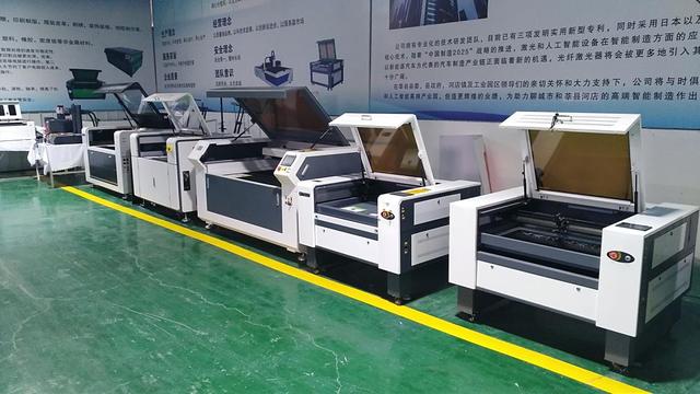
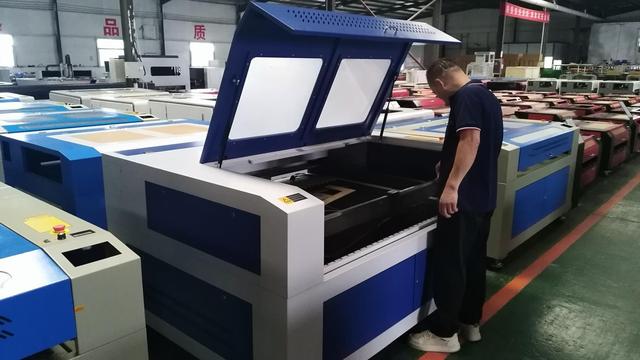
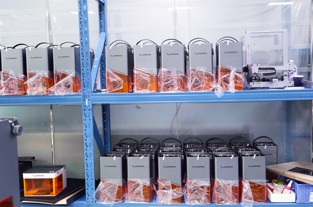
Foshan Stylo Laser Co., Ltd. is a professional manufacturer specializing in advanced industrial laser processing equipment, focusing on ceramic laser cutting machines and silicon steel laser cutting systems. The company is dedicated to delivering high-precision, high-efficiency laser solutions for modern manufacturing industries that require superior accuracy and stable performance.
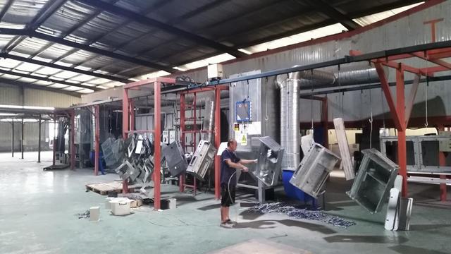
Its core technology is applied in the processing of ceramic materials, electrical steel, and other advanced industrial materials used in transformers, electronics, energy systems, and precision components. By integrating fiber laser technology, CNC control systems, and intelligent automation, Foshan Stylo Laser provides cutting solutions that improve production efficiency while maintaining exceptional cutting quality and minimal material deformation.
The company’s equipment is widely used in industries such as power transmission, semiconductor manufacturing, electrical engineering, and high-end industrial manufacturing. It supports flexible production needs ranging from micro-precision cutting to large-scale industrial processing.
Foshan Stylo Laser Co., Ltd. emphasizes innovation, engineering excellence, and strict quality control. It also provides OEM and ODM customization services to meet diverse global customer requirements. With continuous investment in research and development, the company aims to advance laser processing technology and become a trusted global supplier of precision laser cutting solutions for ceramic, silicon steel, and advanced industrial materials.
Our laser dicing and marking systems are deployed across various critical sectors worldwide:
Precise dicing of SiC MOSFETs for Electric Vehicle inverters, ensuring high reliability in extreme temperature environments.
High-speed dicing for MEMS sensors and mobile phone ICs, where footprint miniaturization is the primary goal.
Utilizing our High-Precision UV Laser Marking for medical device UDI (Unique Device Identification) labels that must withstand sterilization processes.
Processing silicon steel and advanced materials for high-efficiency transformers and grid management systems.